Lijit search

Tuesday, November 30, 2010

General properties of matter

General properties of matter
Elasticity : All most all the substances can be more or less be deformed by applying suitable deforming forces. Some of the substance regain their original shape and size on the removal of deforming force. The property of the substance due to which it regain its original shape and size on the removal of deforming forces is known as elasticity. The substance which completely regain its original shape and size on the removal of deforming forces are known as perfectly elastic but the substance which completely retain its changed dimensions are known as perfectly plastic.

Stress : Whenever a deforming force is applied to bring a change in the dimensions of the substances then the intermolecular force opposes any deformation. This intermolecular force per unit area is known as stress.

In equilibrium the intermolecular force is equal to the applied force. Hence, stress is measured by deforming force per unit area in equilibrium.
Stress= Deforming force/ Area
Types of stress
1. Tensile stress 2. Normal stress & 3. Tangential stress

Strain :The change in dimension per unit original dimension is known as strain.
Types of strain
1. Longitudinal strain 2. volumetric strain & 3. Shear strain.

Sunday, November 28, 2010

FORWARD BAIS & REVERSE BAIS

FORWARD BAIS & REVERSE BAIS
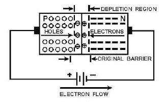
If a battery is connected across a P - N junction with its positive terminal joined to the N - type side and its negative terminal to the p type side, it helps the junction voltage and the junction is said to be REVERSED BAISED. Electrons and holes are repelled further from the junction and the depletion layer winds only a few thermally generated minority carrier cross the junction and a very small current, called reverse current or leakage flows. If a battery is connected across a P - N junction with its positive terminal joined to the P - side and its negative terminal to the N - type side, it opposes the junction voltage and the junction is said to be FORWARD BAISED. Because of the forward baised the depletion layer narrows. When the the battery voltage exceeds the junction voltage and appreciable current flows because majority charge carrier are able to cross the junction, the electrons from N - type side to P - type side and holes in the opposite direction.
In brief a junction conducts when it is forward baised and no current flows through it when it is reversed baised.

P - N JUNCTION

P - N JUNCTION

When a P -type material is placed in contact with an N - type material the contact surface is called P - N junction. As soon as the junction is produced free electrons near the junction in the N - type material move across the junction in the P - type material , where they fill the holes as the result a positive charge is appears near the junction in the N - type material and the negative charge appears in the near the P - type material. At the same time holes diffuse across the junction from the P -type to the N - type material. The exchange of the charge soon stops because the positive charge on the on the N - type side opposes the further flow of holes and the negative charge on the P -type side opposes the further flow of electrons. The region on the either side of the junction becomes fairly free of majority charge carriers and is called depletion layer. The with of depletion layer is of order of 1 micrometer. As the depletion layer builds up a difference of potential appears across the junction because of the positive charge on the N - type side and negative charge on the P -type side. This difference of the potential is called junction voltage or barrier p. d. . At the room temperature the junction voltage is approximately 0.7 V for silicon P- N junction and 0.3 V for Germanium P - N junction.

Friday, November 26, 2010

Formation of P - type semiconductor

P - type semiconductor
A P - type semiconductor is formed when a small amount of trivalent impurity is added to pure Germenium or silicon atom crystal. The addition of trivalent impurity produces a large no. of holes to the host crystals. To explain the formation of P - type semiconductor, let us introduce a trivalent impurity into the lattice of a pure silicon crystal. The trivalent atom has 3 valance electrons and form covalent bonds with neighbouring atoms. The 4th bond is incomplete . the trivalent atom then attracts an electron from an adjacent atom there by completing the 4th bond and forming a hole in the adjacent atom. Since a trivalent impurity atom provides 1 hole, an enormous increase occurs in the number of holes. The impure crystals so obtained is called P - type semiconductor where P represents the positive charge on hole. Thus the majority carrier in a P - type semiconductor are holes. Free electrons are also present in the P - type semiconductor. These are thermally generated and since they relatively few, they are called minority carriers. The trivalent impurity atoms are called acceptors because each accepts an electron when the atom is introduced into the host crystal.

Formation of N - type semiconductor

Formation of N - type semiconductor
An N - type semiconductor is formed when a small amount of pentavalent impurity is added to a pure Germenium or Silicon crystal. The addition of pentavalent impurity produces a large no. of free electrons in the host crystal.
To explain the formation of N - type semiconductor, let us introduce a pentavalent impurity atom into the lattice of pure silicon crystal. The pentavalent atom has 5 valance electrons, but only 4 form covalent bonds with the neighbouring atoms. The 5th electron finds no place in the covalent bonding so becomes free. Since an impurity atom provides one free electron, an enormous increase occurs in the no. of free electrons. The impure semiconductor so obtained is then called as N - type semiconductor where N represents negative charge on an electron. Thus the majority carrier in N - type semiconductor are free electrons. Holes are also present in the N - type semiconductor. These are thermally generated and since they are relatively few, they are called minority carrier.
The pentavalent impurity atom are called donour because each donate a free electron to the host crystal.

Thursday, November 25, 2010

Semiconductors contd.......

Semiconductors contd.......
For metals, the valance and conduction bands can overlap. The electrons in the overlapping region of energy are conduction electrons. Since there is large number of conduction electrons, the metals are good conductors.
An intrinsic semiconductor is a pure semiconductor. for instance, a silicon crystal is an intrinsic semiconductor if energy energy atom in the crystal is silicon atom.
A pure semiconductor has a very small electrical conductivity at ordinary temperature however, its conductivity can be increased appreciably by adding a small amount of trivalent impurity or pentavalent impurity to it. The process of adding the impurity is called DOPING. & the impurity is called dopant. The semiconductors so obtained is called extrinsic semiconductor.
When a pentavalent impurity is added to a pure semi conductor crystal during a crystal growth, the resulting semiconductor crystal is called N- semiconductor.
When a trivalent impurity is added to a pure semiconductor crystal during crystal growth, the resulting semiconductor crystal is called a P- semiconductor.

Semiconductors

Semiconductors id=
A semiconductor is a material whose conductivity lies between that of good conductor & good insulator . Silicon and germanium are the examples of semiconductors widely used in the electronics industry .
According to the band theory, semiconductors are a class of material in a narrow forbidden band. The energy gap is the order of 1 eV . At absolute zero, the valance band energy levels are completely filled by by electrons, the conduction band is empty, & the material is then an insulator. At normal temperature, the thermal energy of some electrons is sufficient for them to reach the conduction band, where they become conduction electrons. The gap left in the valance band by the movement of an electron is called a HOLE. A hole acts as if it were positively charged carrier . Both hole and conduction electrons take part in electrical conduction in a semi conductor.
In insulators, the valance band is energy is completely filled by electrons. The conduction band is empty but the two bands are separated by a wide energy gap (6-9 eV ), called forbidden band. Under an applied electric field, the valance electrons cannot gain enough energy to jump to the conduction band. so, the material is insulator.

Twitter Delicious Facebook Digg Stumbleupon Favorites More

 
Powered by Blogger