Lijit search

Showing posts with label Modern physics. Show all posts

Friday, November 26, 2010

Formation of P - type semiconductor

P - type semiconductor
A P - type semiconductor is formed when a small amount of trivalent impurity is added to pure Germenium or silicon atom crystal. The addition of trivalent impurity produces a large no. of holes to the host crystals. To explain the formation of P - type semiconductor, let us introduce a trivalent impurity into the lattice of a pure silicon crystal. The trivalent atom has 3 valance electrons and form covalent bonds with neighbouring atoms. The 4th bond is incomplete . the trivalent atom then attracts an electron from an adjacent atom there by completing the 4th bond and forming a hole in the adjacent atom. Since a trivalent impurity atom provides 1 hole, an enormous increase occurs in the number of holes. The impure crystals so obtained is called P - type semiconductor where P represents the positive charge on hole. Thus the majority carrier in a P - type semiconductor are holes. Free electrons are also present in the P - type semiconductor. These are thermally generated and since they relatively few, they are called minority carriers. The trivalent impurity atoms are called acceptors because each accepts an electron when the atom is introduced into the host crystal.

Formation of N - type semiconductor

Formation of N - type semiconductor
An N - type semiconductor is formed when a small amount of pentavalent impurity is added to a pure Germenium or Silicon crystal. The addition of pentavalent impurity produces a large no. of free electrons in the host crystal.
To explain the formation of N - type semiconductor, let us introduce a pentavalent impurity atom into the lattice of pure silicon crystal. The pentavalent atom has 5 valance electrons, but only 4 form covalent bonds with the neighbouring atoms. The 5th electron finds no place in the covalent bonding so becomes free. Since an impurity atom provides one free electron, an enormous increase occurs in the no. of free electrons. The impure semiconductor so obtained is then called as N - type semiconductor where N represents negative charge on an electron. Thus the majority carrier in N - type semiconductor are free electrons. Holes are also present in the N - type semiconductor. These are thermally generated and since they are relatively few, they are called minority carrier.
The pentavalent impurity atom are called donour because each donate a free electron to the host crystal.

Thursday, November 25, 2010

Semiconductors contd.......

Semiconductors contd.......
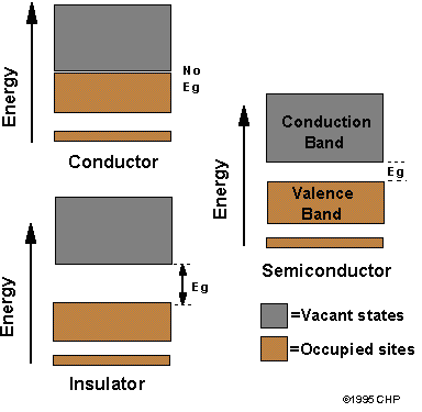
For metals, the valance and conduction bands can overlap. The electrons in the overlapping region of energy are conduction electrons. Since there is large number of conduction electrons, the metals are good conductors.
An intrinsic semiconductor is a pure semiconductor. for instance, a silicon crystal is an intrinsic semiconductor if energy energy atom in the crystal is silicon atom.
A pure semiconductor has a very small electrical conductivity at ordinary temperature however, its conductivity can be increased appreciably by adding a small amount of trivalent impurity or pentavalent impurity to it. The process of adding the impurity is called DOPING. & the impurity is called dopant. The semiconductors so obtained is called extrinsic semiconductor.
When a pentavalent impurity is added to a pure semi conductor crystal during a crystal growth, the resulting semiconductor crystal is called N- semiconductor.
When a trivalent impurity is added to a pure semiconductor crystal during crystal growth, the resulting semiconductor crystal is called a P- semiconductor.

Semiconductors

Semiconductors id=
A semiconductor is a material whose conductivity lies between that of good conductor & good insulator . Silicon and germanium are the examples of semiconductors widely used in the electronics industry .
According to the band theory, semiconductors are a class of material in a narrow forbidden band. The energy gap is the order of 1 eV . At absolute zero, the valance band energy levels are completely filled by by electrons, the conduction band is empty, & the material is then an insulator. At normal temperature, the thermal energy of some electrons is sufficient for them to reach the conduction band, where they become conduction electrons. The gap left in the valance band by the movement of an electron is called a HOLE. A hole acts as if it were positively charged carrier . Both hole and conduction electrons take part in electrical conduction in a semi conductor.
In insulators, the valance band is energy is completely filled by electrons. The conduction band is empty but the two bands are separated by a wide energy gap (6-9 eV ), called forbidden band. Under an applied electric field, the valance electrons cannot gain enough energy to jump to the conduction band. so, the material is insulator.

Twitter Delicious Facebook Digg Stumbleupon Favorites More

 
Powered by Blogger